SPI (Serial Data Transfer)
A SPI Interface can be:
- Simplex: Only unidirectional
- Half-duplex: Bidirectional, but only in one direction at a time
- Full-duplex: Bidirectional, both directions simultaneously
The timing component of an SPI bus can be:
- Asynchronous: Each node uses an individual clock
- Synchronous: All nodes use the same clock signal generated by the master
In SPI, it is configurable if the MSB or LSB is sent first.
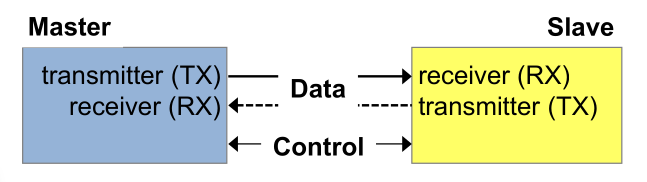
Data Connections
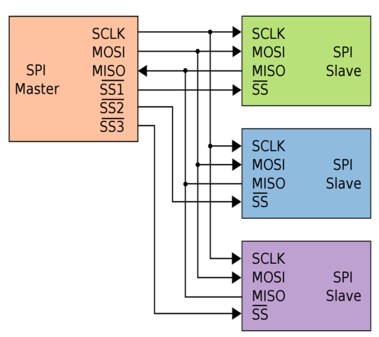
SPI is full duplex and has to following lines:
- MOSI (Master-out-Slave-in): Data from master to slave
- MISO (Master-in-Slave-out): Data from slave to master
- SSx (Slave Select): The master sets the SS to
0to initiate the data transfer. Each slave needs its ownSSxline.
Implementation
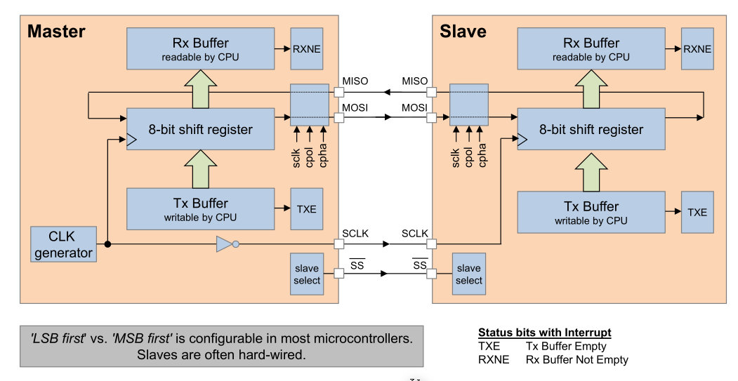
The shift register are 8 flip-flops which are chained together. Each clock cycle the input signal is stored in the first flip-flop, the data of the first flip-flip is written to the second flip-flip, etc. After 8 clock cycles the whole 8-bit shift register was overwritten.
Importantly, data is always sent and received simultainously.
The clock signal of the master is inverted. This was done to help with the inherit timing issue that long lines can create. This way, the flanks are effectively sent a half-flank earlier.
For the CPU the Rx-Buffer and Tx-Buffer are at the same address.
Flags/Interrupts
The following flags generate interrupts
- TXE: TX-Buffer empty The CPU had wrote some data to the TX-Buffer which was sent out
- RXNE: RX-Buffer not empty Data was received and the CPU can access it
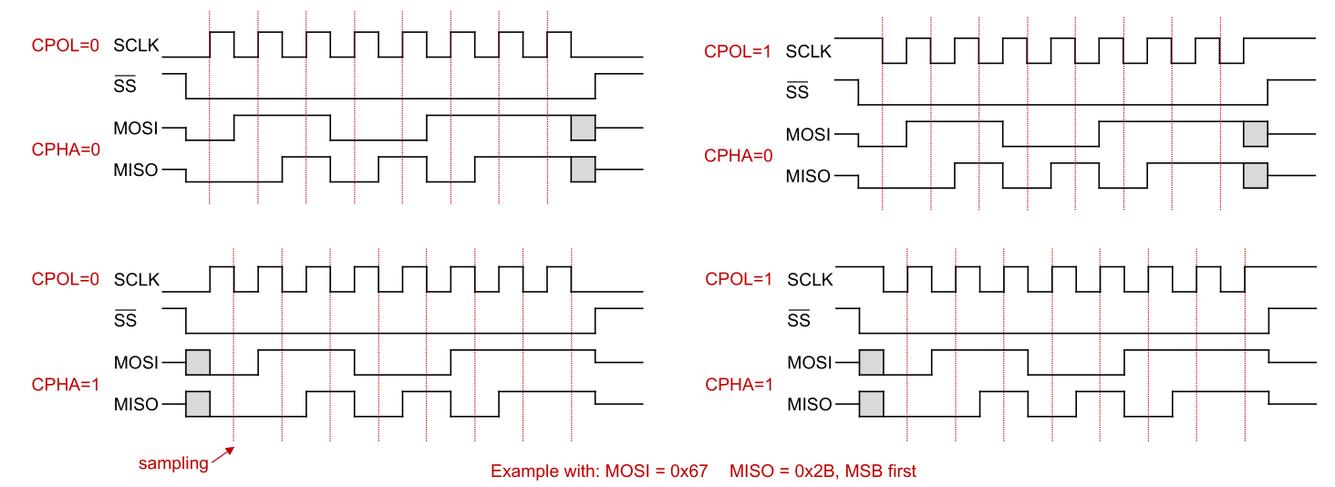
Timing
The data is read on the sampling edge of the clock. The data can change on the toggling edge. Which edge (raising or falling) is which edge, can be configured in the CPU.
- CPOL (Clock Polarity): Where the clock rests, when nothing is transmitted
- CPHA (Clock Phase): If set to
0, then the first edge (rasing or falling) is the sampling edge. On the other hand, ifCPHAis set to1, then the second edge is the sampling edge.
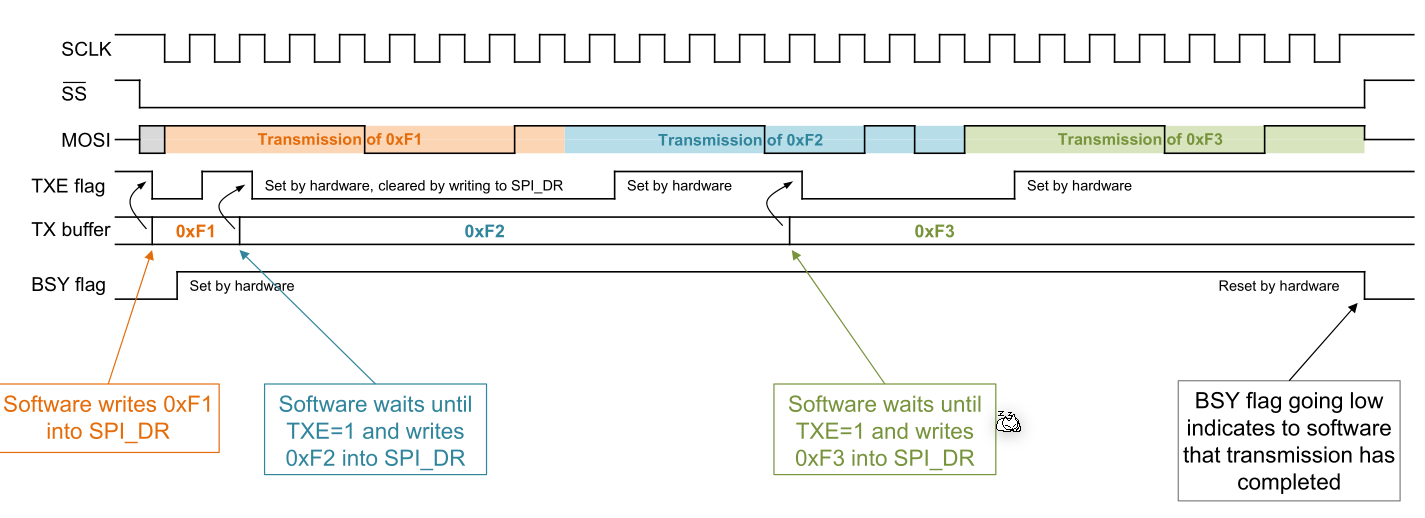
In the following diagram, the internal communication in the CPU, when transmitting three bytes, is displayed. Interesting enough, the TXE flag is set to 1 again way earlier than it is actually sent. This is done to relieve the CPU, because as soon the SPI chip copied the TR-buffer to its internal button, the CPU can write another byte into it.
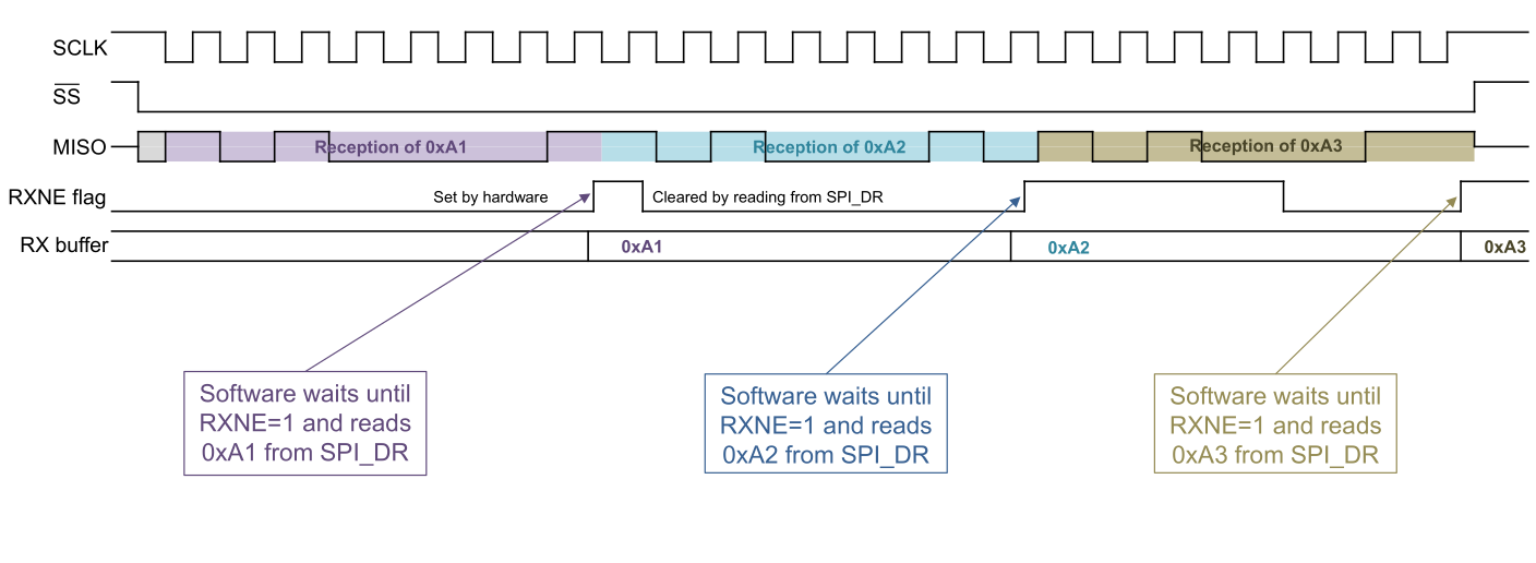
It works similarly when the CPU receives data.
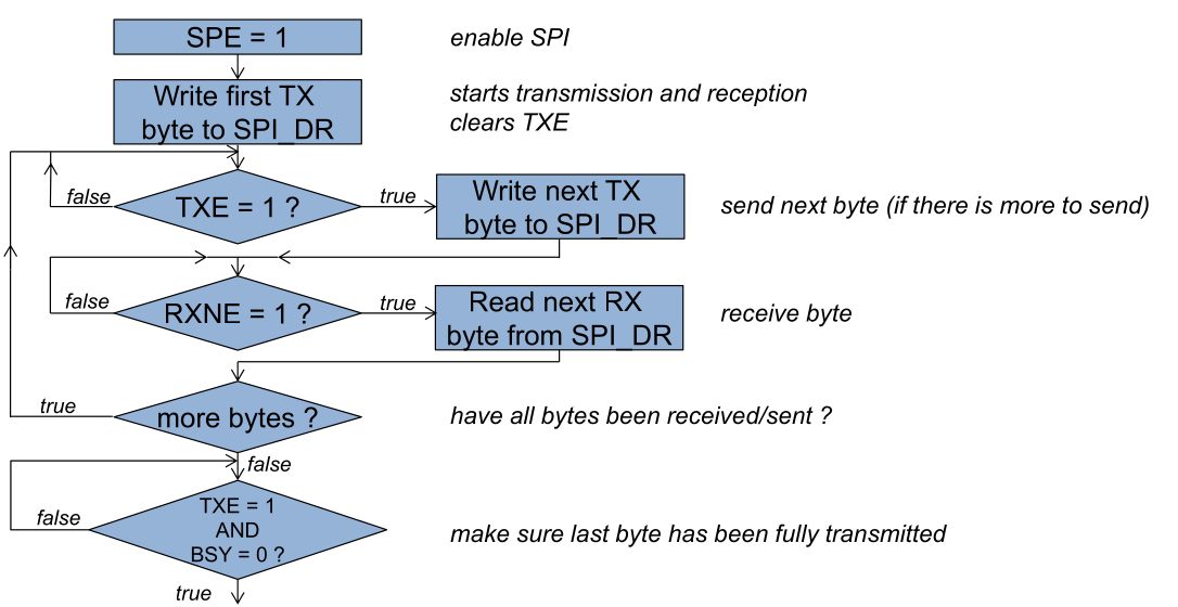
The following flow can be used to simultaneously read and write from a SPI device. Alternatively interrupts, which are generated when TXE and RXNE change to 1, can be used.
Implementation on the STM32F4xxx
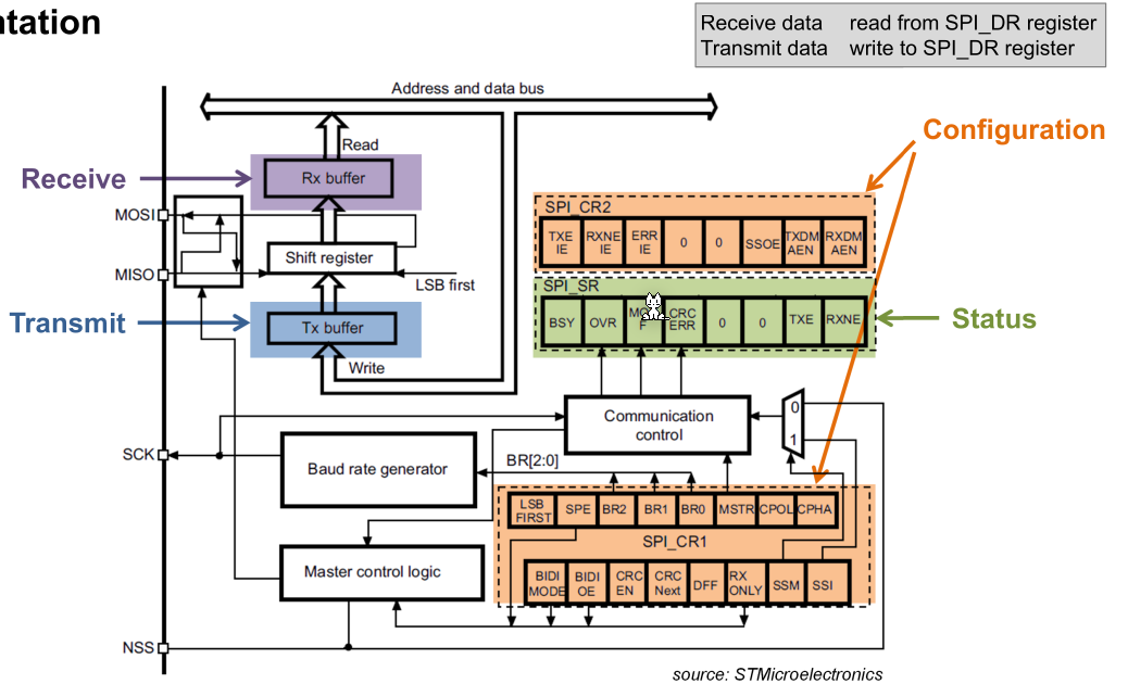
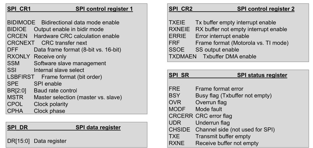
- Control Register
- MSTR (Master): If set to
1then the CPU is a master, otherwise a slave - BR0-2: Used to set the baud rate
- CPOL (Clock Polarity): Where the clock rests, when nothing is transmitted
- CPHA (Clock Phase): If set to
0, then the first edge (rasing or falling) is the sampling edge. On the other hand, ifCPHAis set to1, then the second edge is the sampling edge. - Status Registers
- BSY (Busy): If set, then the SPI chip is busy
- OVR (Overrun): If the CPU doesn't read data fast enough and a new byte already arrived, then the data register is overwritten and the
OVRbit is set. - TXE (TX-Buffer empty): The CPU had wrote some data to the TX-Buffer which was sent out
- RXNE (RX-Buffer not empty): Data was received and the CPU can access it