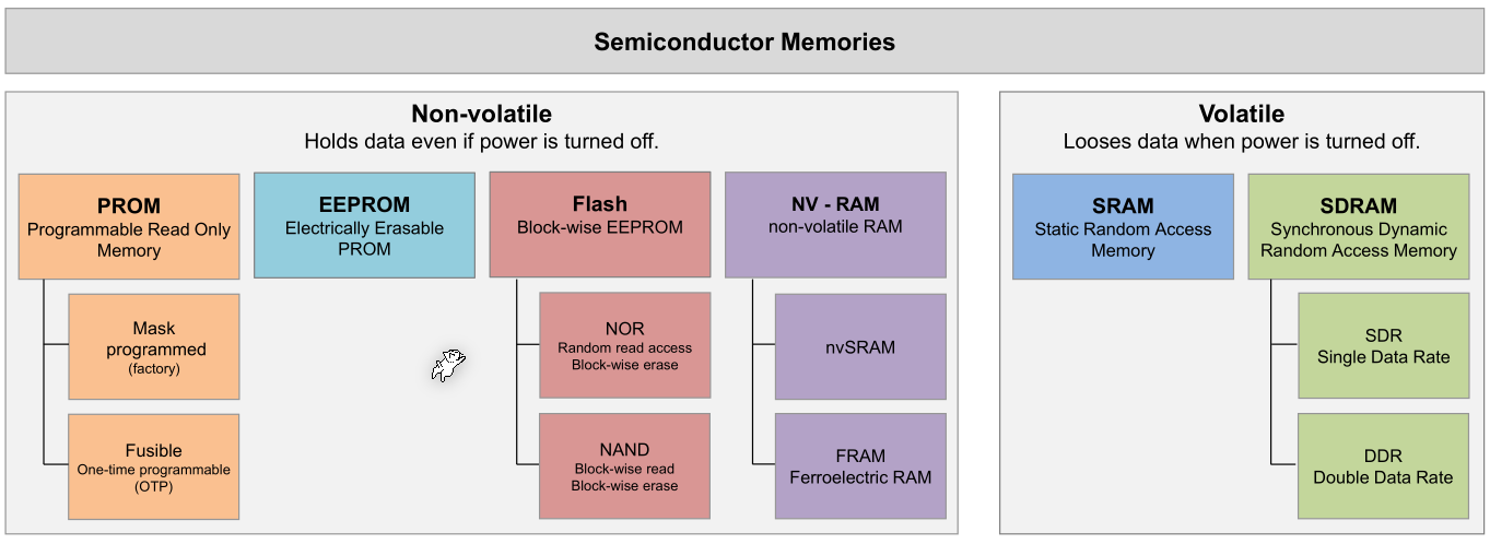
Memory
Memory Cell
One memory cell is a transistor which can pull down the bit line, if "set". This means a transistor is by default 1, and only if programmed can become a 1.
ROM
Programmable Read-Only Memory (PROM)
This kind of memory can only be written to once by burning fuses. When the fuse is burnt, the data line will be 1. Otherwise, if not burn, then the data line will be 0.
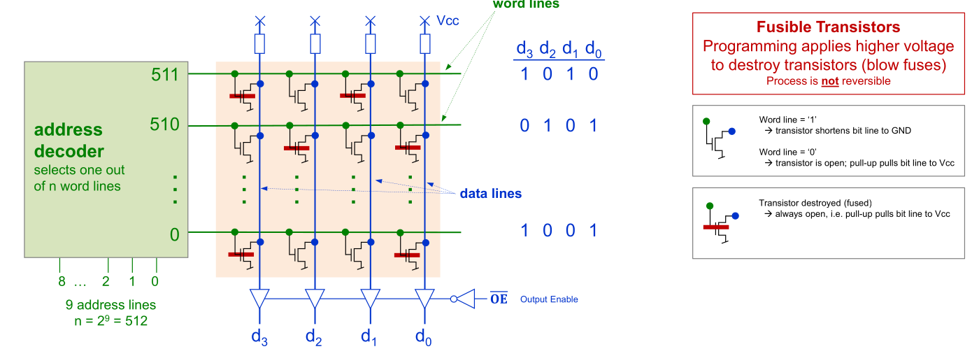
In addition, see diagram below.
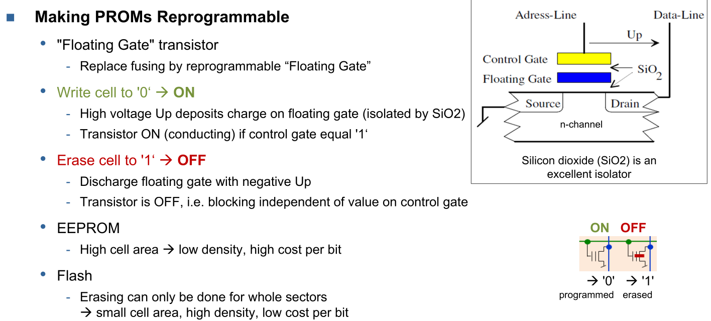
Floating Gate Memory
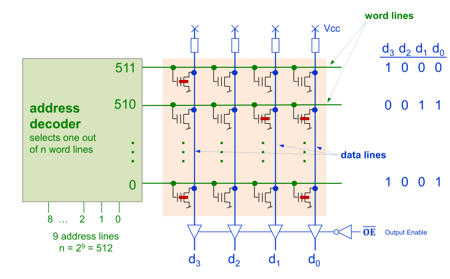
Memory cells are organised in a grid:
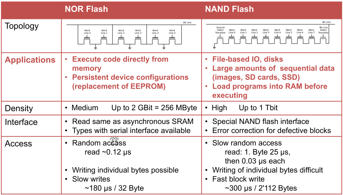
NOR and NAND Flash
RAM
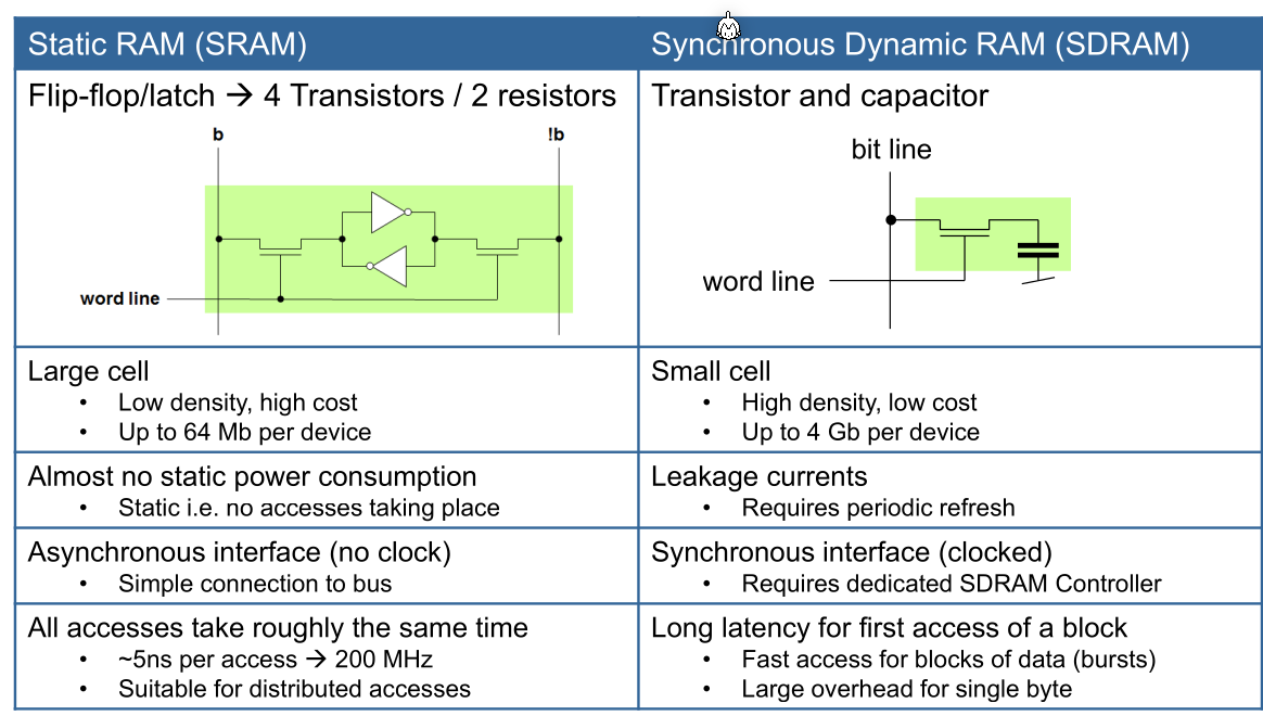
Static Random Access Memory (SRAM)
(Has an asynchronous interface/without a clock)
SRAM has the following advantages and disadvantages:
- All accesses take roughly the same time, independent of what was previously read/written or the location
- No refreshs are needed
- Memory is volatile
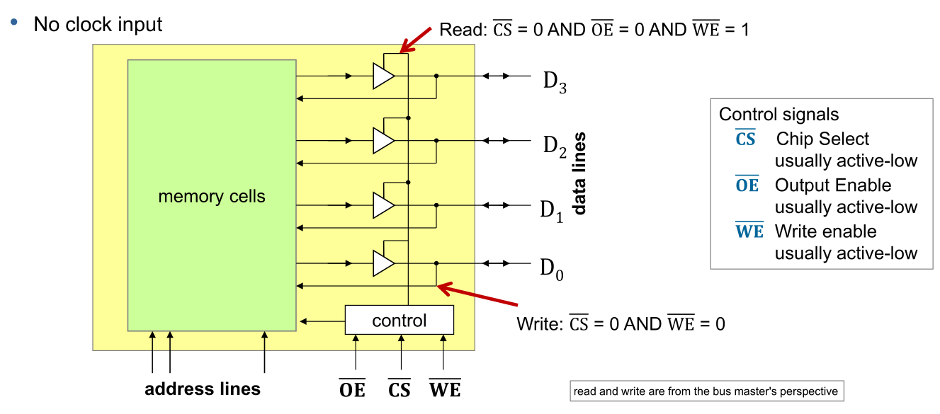
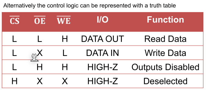
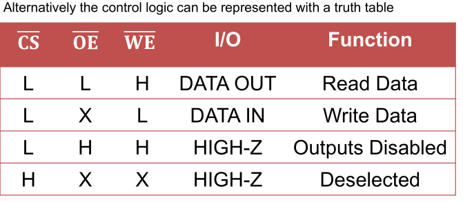
(X=don't care, L=low, H=high)
The control lines are active-low, meaning that L=enabled and H=disabled
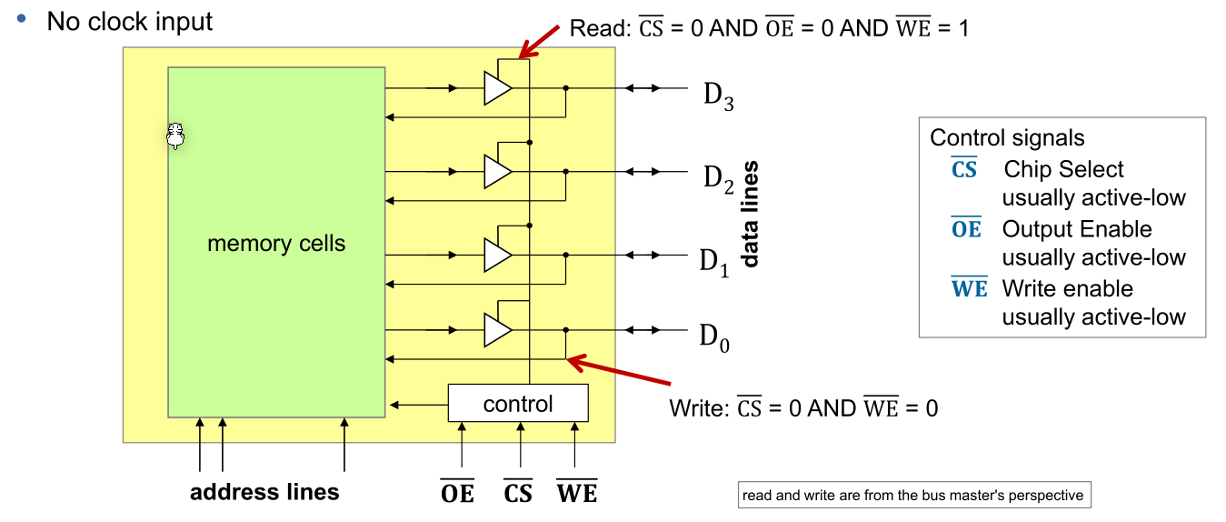
The following shows the internal of SRAM:
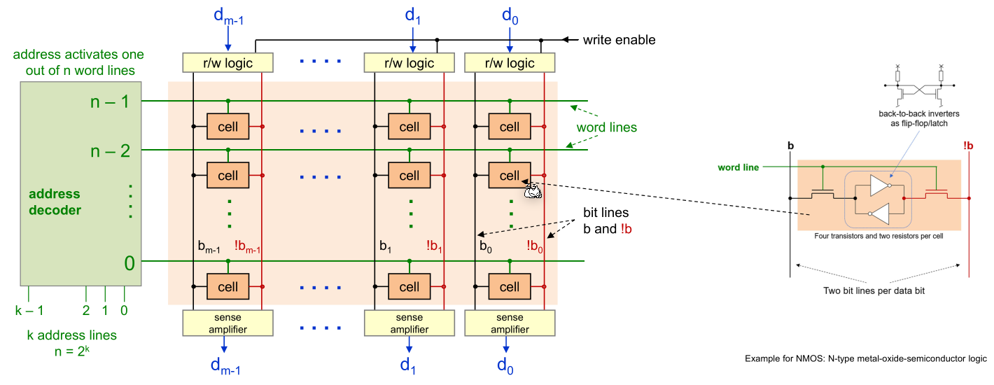
SRAM uses a stable circuit which "self-confirms". This can be easily be archived by chaining two inverters.
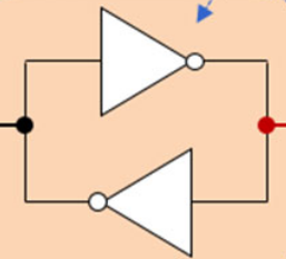
To override such a circuit, one has to apply a high voltage current (a 1 to one side and a 0 to the other side). Because of the high voltage, this will overpower the inverters and overwrite their value.
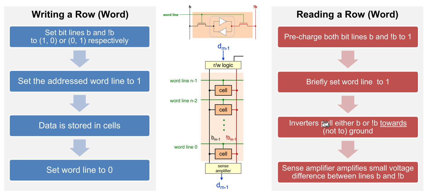
The following steps explain how to write and read an SRAM cell.
Synchronous Dynamic Random Access Memory (SDRAM)
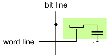
SDRAM uses a capacitor as a battery to store the individual bits. However, capacitor loos their charge over time and thus the RAM controller needs to periodically read and immediately write the value back to recharge the capacitor.
The following diagram shows the layout of a SDRAM chip.
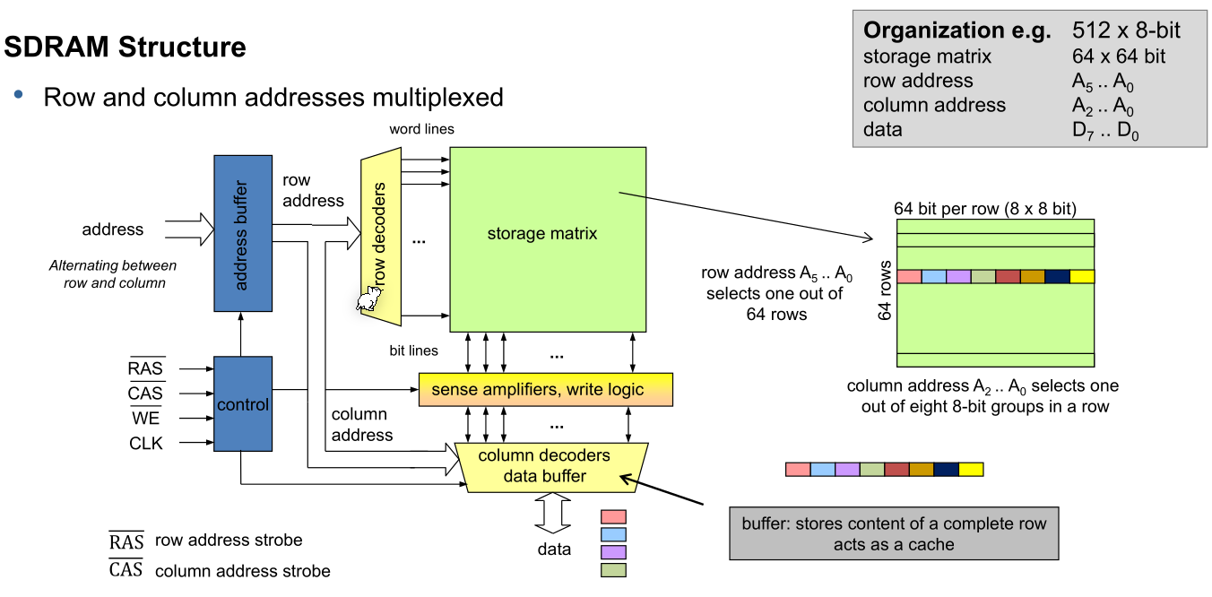
Compared to SRAM, SDRAM has a lot wider storage matrix. This makes the refreshing faster, but also more complicated.
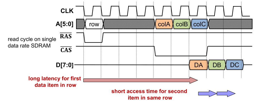
To access a byte in SDRAM, the FMC/CPU first enables not RAS (row address strobe) by writing 0 and sending the row address. When not RAS is zero, the address is sent to the row decoder. Then not CAS is set to 0 which causes the next address being sent to the column decoder.
For the first byte, the SDRAM needs a lot of cycle, but further bytes in the same row are really fast as the row is already "loaded". This makes this storage technology not appropriate for direct CPU access. To still be able to use DRAM, the CPU has caches which are a lot faster and more predictable.
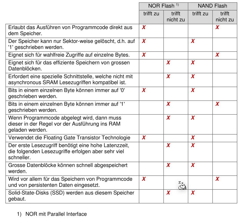
Comparison:
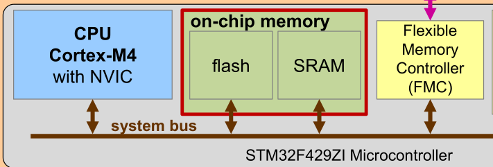
STM32F429ZI
The following shows the simplified architecture of the STM32F429ZI:
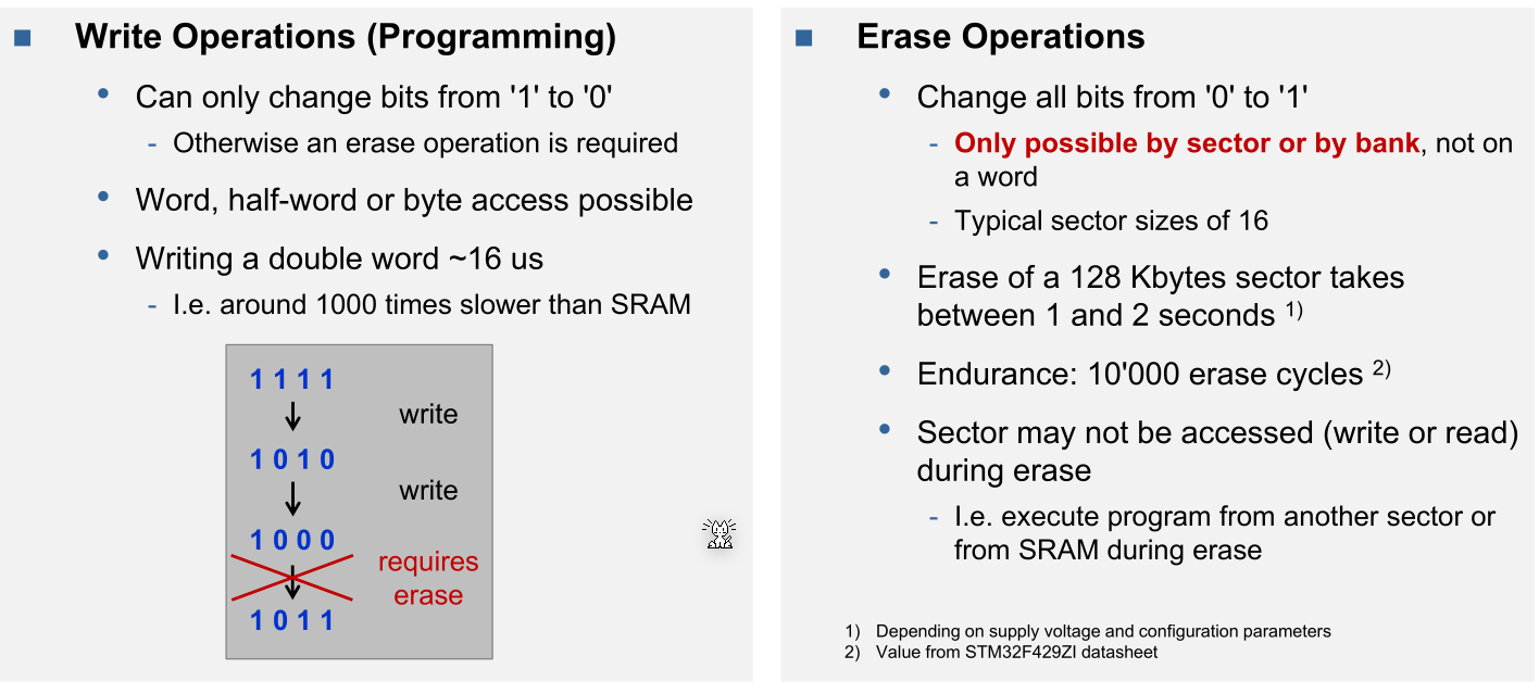
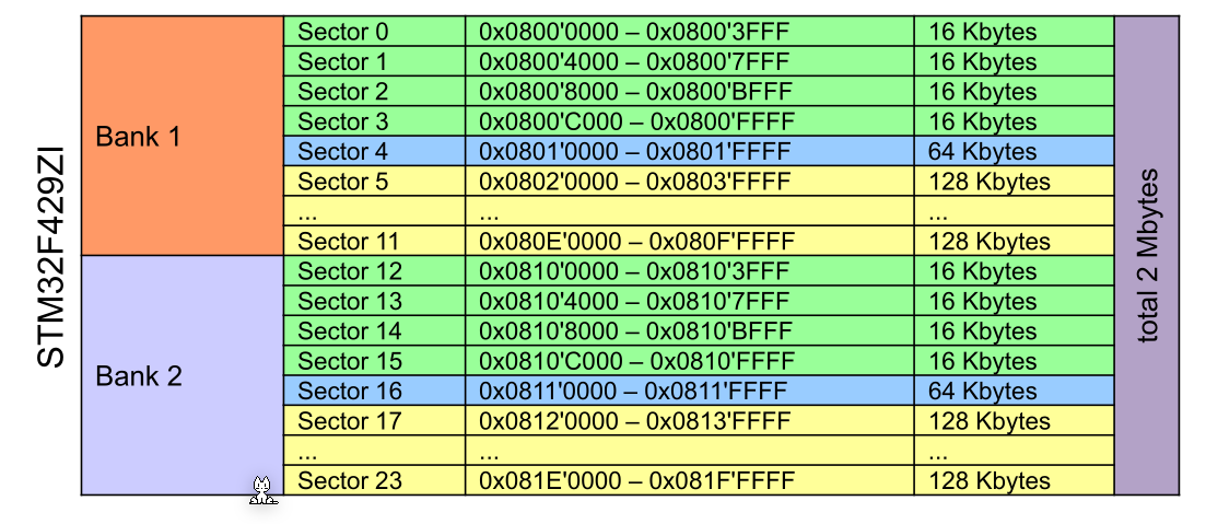
Sectors can only be erased as a whole.
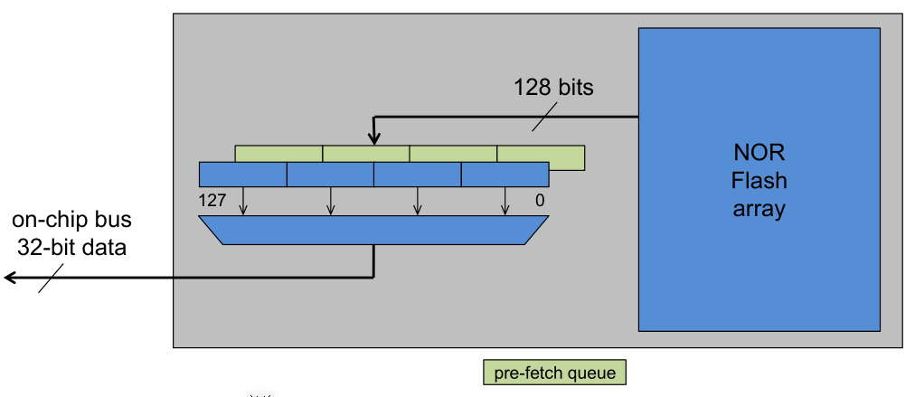
The flash has a 128bit buffer in front, which pre-fetches the next instructions. This minimises the latency of flash.
Flexible Memory Controller (FMC)
The FMC allows a programmer to specify how external memory is mapped to the CPU.
The FMC is a slave on the system bus and a master on the external bus.
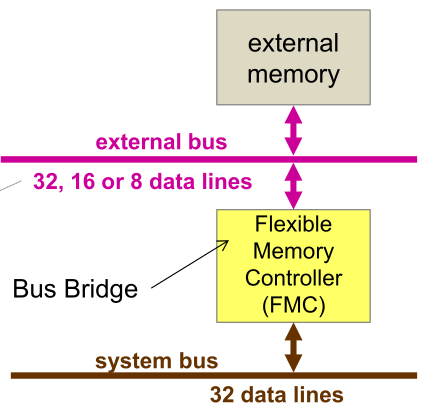
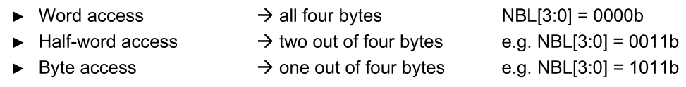
The external bus has a 26-bit address bus with 8, 16 or 32 bit data lines.
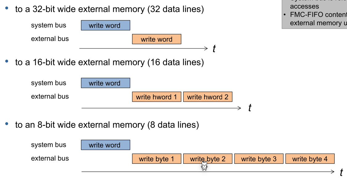
If the FMC needs to translate a 32-bit bus to a lower bit bus (e.g. 16bit or 8bit bus) then the FMC needs to write multiple data packages. The FMC caches the data, meaning that while the FMC is writing, the CPU and system bus can do something else.
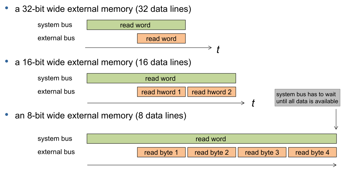
If reading, the CPU and system bus need to wait for the external read to finish.
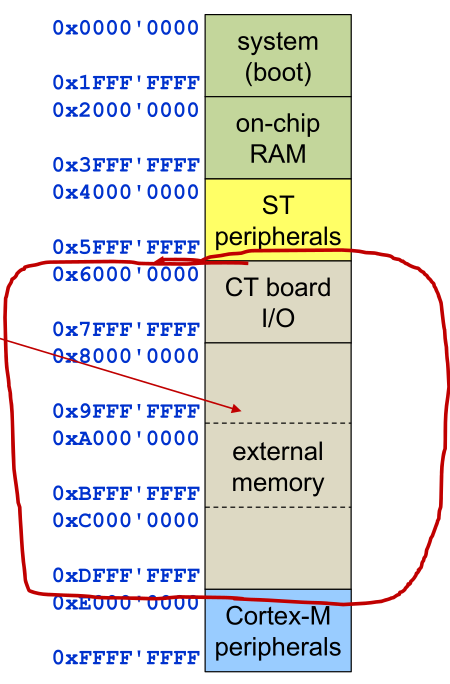
The FMC controls the following memory area:
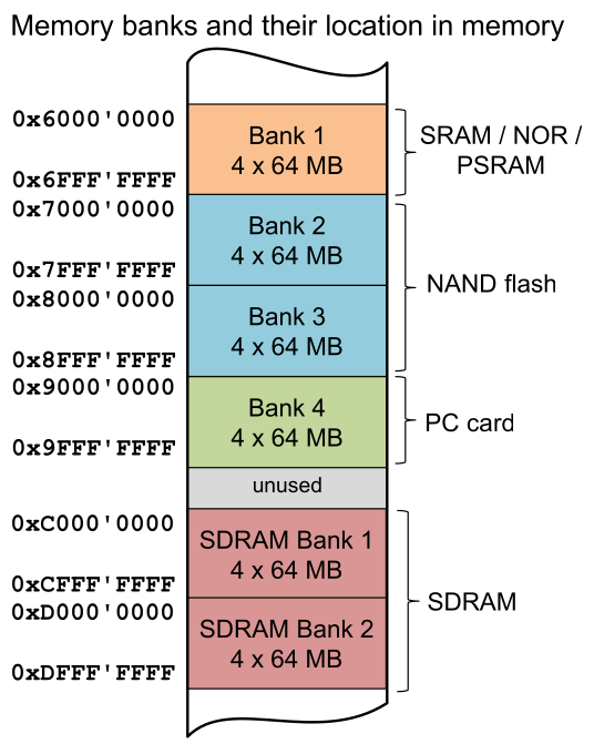
Each bank are designed for different kind of memory. The FMC will produce different electrical signals for different "bank types".
Each bank can have 4 devices connected.
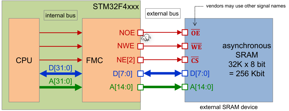
Bank 1 (SRAM, NOR, PSRAM)
The following shows a schematic of the wiring of bank 1:
The following truth table shows the selected functionality when different pins are high/low.
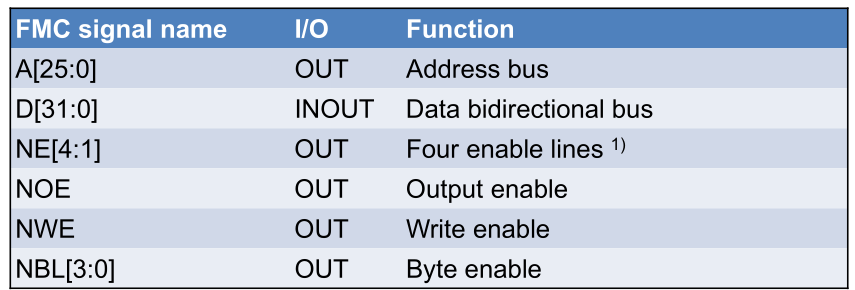
The following table shows the inputs and outputs of the FMC:
The FMC is connected in the following way:
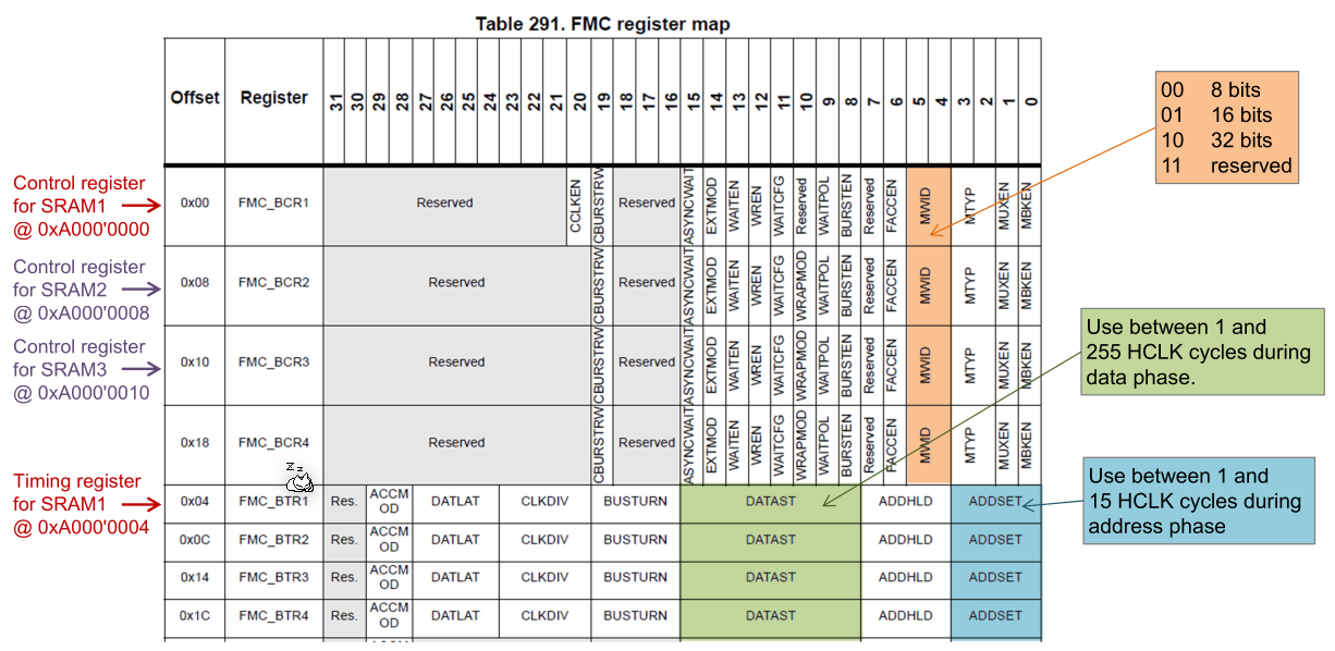
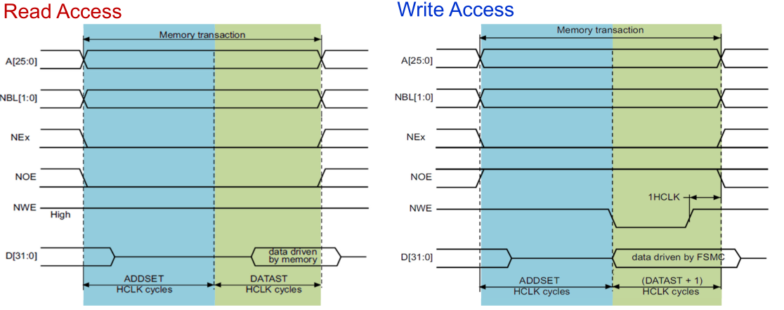
The following configuring options exist:
HCLK is the clock cycle of the CPU and the internal bus and is configured to 82 MHz during the startup of the CT board.